Lattice LCMXO2-2000HC-5MG132I: A Comprehensive Technical Overview of Low-Power FPGA Capabilities and Applications
The Lattice Semiconductor MachXO2 series represents a significant milestone in the evolution of low-power, low-cost FPGAs, and the LCMXO2-2000HC-5MG132I is a prominent member of this family. This device encapsulates a powerful blend of programmability, efficiency, and integration, making it an ideal solution for a vast array of modern electronic applications. This article provides a detailed technical overview of its architecture, key features, and primary use cases.
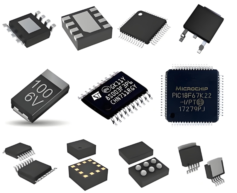
At the core of the LCMXO2-2000HC-5MG132I is a non-volatile, flash-based FPGA fabric. This technology is fundamental to its value proposition, offering instant-on operation and high security, as the configuration is inherent to the chip and cannot be easily read back. The "2000" in its name denotes 2280 Look-Up Tables (LUTs), providing a substantial logic capacity for implementing complex control logic, state machines, and data path management. The device is packaged in a 132-ball, 0.5mm pitch, Micro-BGA (5MG132I), which is suited for space-constrained PCB designs.
The defining characteristic of this FPGA is its ultra-low power consumption. Operating from a single 3.3V or 2.5V supply with 1.2V core voltage, it boasts a static power consumption as low as 19 µW. This makes it exceptionally suitable for battery-powered and portable devices where energy efficiency is paramount. Furthermore, it features up to five user-programmable low-power modes, allowing designers to finely tune the balance between performance and power dissipation dynamically.
Beyond the core logic, the LCMXO2-2000HC is richly equipped with embedded hard IP blocks. This includes:
Embedded Block RAM (EBR): 56 Kbits of sysMEMORY™ EBR for efficient data buffering and storage.
Embedded User Flash Memory (UFM): 64 Kbits of dedicated flash, perfect for storing user data, system parameters, or even soft microcontroller code.

Pre-Engineered Source Synchronous I/O: Support for numerous interfaces including I²C, SPI, and LED drive is built-in, simplifying the connection to common peripherals and sensors.
These features drastically reduce the need for external components, lowering the total system cost and board space.
The combination of low power, small form factor, and integrated features opens a wide spectrum of applications. Key areas include:
System Management: It is perfect for power sequencing, voltage monitoring, and acting as a "Green-Glue" logic component to offload tasks from a primary processor or microcontroller unit (MCU).
Communications Bridge: The FPGA can seamlessly translate between different voltage levels and protocols (e.g., SPI to I²C, GPIO expansion), resolving interface incompatibilities between system components.
Sensor Aggregation and Control: In IoT endpoints, it can manage multiple sensors, perform preliminary data processing, and control wireless communication modules, significantly extending battery life.
Consumer Electronics: Used in smartphones, tablets, and wearables for functions like power management, touch screen controller interfacing, and LED control.
ICGOOODFIND: The Lattice LCMXO2-2000HC-5MG132I stands out as a highly versatile and efficient programmable logic solution. Its flash-based instant-on operation, remarkably low static power, and high integration of essential system functions make it a superior choice for designers aiming to reduce system cost, power, and size without compromising on flexibility or performance. It successfully bridges the gap between discrete logic, ASSPs, and more expensive, higher-power FPGAs.
Keywords: Low-Power FPGA, Flash-Based, Embedded Block RAM, System Management, Green-Glue Logic
